Enabling the rapid production of printed electronics with nanomaterial inks
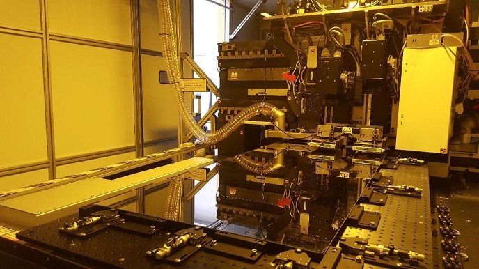
Printed electronics (PE) holds out the promise of revolutionising the electronics industry, due to its ability to print nanomaterials directly onto surfaces. These nanomaterials can have conductive, resistive, capacitive and semi-conducting properties. Compared to traditional circuit board and semiconductor manufacturing techniques, PE offers cost, performance and environmental advantages. The EU-funded INSPIRED (INdustrial Scale Production of Innovative nanomateRials for printEd Devices) project was set up to further develop the nanomaterial printing technology to meet growing demand. The EU-funded project conducted pilots for silver nanowires and graphene production, and has brought new products based on formulations of these materials to market. The quest to develop suitable nanomaterials Compared to current circuit board and semiconductor manufacturing techniques, PE is more cost-effective, is capable of operating at higher volume and is more environmentally friendly. However, if there is going to be significant migration towards liquid-based, high-throughput PE systems, suitable ink-based nanomaterials will need to be developed and available in industrial quantities. These will also have to meet the relevant industrial standards and be compatible for end user applications. Project coordinator Mr Andreas Rudorfer adds the caveat that, “PE is often considered as a full replacement of the semiconductor industry but that is not the case. It is a supplement for certain applications and markets where the benefits of PE show their full potential, such as the display market.” INSPIRED set out to develop and demonstrate high-volume printing of nanomaterials for printed electronics such as: solar cells (copper indium gallium selenide photovoltaics (CIGS PV)), capacitive touch screens (CTS) and liquid crystal displays (LCD). INSPIRED developed two pilot lines to determine nanomaterial characterisation, both of which progressed at a very fast pace. Silver nanowires were synthesised using wet chemical reduction processes, while graphene nanoplatelets were optimised using large-scale exfoliation production. In terms of formulation, silver nanowires were created and were suitable for use in high-volume spray deposition processes. Graphene nanoplatelets were developed and were capable of providing enhanced properties when combined with the silver nanowires. “Nanosafety aspects of materials and processes have been considered throughout, ensuring safe handling with substances of concern. To achieve a project-tailored approach, a nano-related safety strategy, in accordance with REACH, has been developed,” says Rudorfer. Towards achieving a volume processing, high-speed, ink-jet printing system, the consortium’s equipment manufacturer built a ‘Large Area Print and Laser Sinter Tool’ capable of handling substrates up to 1.11 x 1.3 m for industrial applications. Of strategic importance to the EU economy The INSPIRED project is an industry-driven Research and Innovation Action that supports the objectives and vision of the Horizon 2020 Industrial Technologies Programme, by increasing the nanotechnology base of EU manufacturers. As Rudorfer says, “INSPIRED will have a positive impact across the entire value chain of the PE sector, benefiting nanomaterial suppliers, ink manufacturers, printing companies, equipment suppliers and the high-value manufacturing sectors in general.” The materials and processes developed by the project are already leading to new and enhanced products. For example, project partner Thomas Swan has developed a pilot line for graphene nanoplatelets and products (under the brand name Elicarb®) which are already being sold to industry manufacturers and component users alike. To take the work forward, the INSPIRED team is assessing the pilot lines for upscaling potential, and will upgrade or replace production processes as required to meet manufacturing requirements and market expectations.
Keywords
INSPIRED, printed electronics, nano, ink, manufacturing, graphene, LCD, capacitive touch screens, solar cells, circuit boards, nanosafety, nanomaterial