Less expensive electrical connections
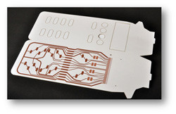
Small and medium-sized enterprises (SMEs) active in the printed electronics field traditionally make their inks from silver nanoparticles. The raw material and its processing costs are quite high, accounting for nearly half of overall product costs. Researchers on the EU-funded 'Enhancing printed electronics applications by SMEs' (CLIP) project focused on lowering the costs associated with devices employing conductive inks. Investigators developed inexpensive conductive inks from mixtures of low-cost copper flakes and a small amount of copper nanoparticles for screen printing and flexography printing. Photonic sintering or curing was used to expedite the processing speed and facilitate the development of products for markets otherwise not accessible. Photonic sintering is a high-temperature process using pulsed light rather than constant heat as in an oven. It enables significantly higher temperatures than a substrate could normally withstand, expanding possible substrates to flexible and inexpensive plastic or paper. Photonic sintering of the low-cost copper inks resulted in comparable performance (surface resistances) in electroluminescent (flat panel) displays and intelligent packaging relative to thermal-sintered thick-film silver inks. Scientists estimated that the end-user cost of the inks would be reduced by at least 50 %. Further, the technologies pave the way to previously inaccessible markets, including ultra-high-frequency radio frequency identification (RFID) devices that facilitate readability at long distances. The team also developed inks for inkjet and aerosol-jet printing made of silver nanoparticles of various sizes (multimodal size distribution), including 2 particle sizes much smaller than the reference 40 nm. The smaller particles sinter at lower temperature, making a denser structure with higher conductivity at the same sintering temperature compared to a unimodal distribution. This means that materials thickness and associated costs can be reduced for the same conductivity. The multimodal inks were demonstrated in new applications, including inexpensive chip-less RFID tags and smart packaging sensors. As promised, CLIP delivered two inexpensive alternatives to conventional silver nanoparticle conductive inks for printed electronics. The copper-based formulations and the multimodal silver ones could lower the costs of inks by 40-50 % while opening the door to new markets for the SMEs that produce them.