Recycling silicon dust to reduce solar panel waste
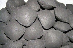
Silicon wafers – ultrathin semiconductors used in the manufacture of solar panels ̶ are produced by slicing large silicon blocks. But the process is wasteful, with as much as 50 % of the valuable original material lost as fine silicon powder during the industrial sawing process. EU funded researchers under the SIKELOR(opens in new window) project have been looking at ways to recycle the silicon dust and so reduce waste in an industry already under pressure from cheap producers outside Europe. ‘The thickness of the silicon wafer is in the order of around 10 to 20 microns and the thickness of the sawing wire is almost the same. That means about half of the material remains as sawing loss,’ says project coordinator Sven Eckert, a physicist at the Heimholtz Centre Dresden-Rossendorf(opens in new window). The main goal of the team, made up of both academics and industry researchers, was to develop a single process to compact and melt the expensive silicon waste and separate the impurities so that it can be reused in solar panel manufacture. ‘Impurities reduce the efficiency of solar panels. You want very clean materials at the end of the recycling process,’ Dr Eckert says. Compacting and melting The team first developed a process for compacting the fine powder into pellets. But this ‘is not so straightforward’, Dr Eckert notes, as the tiny particles present a risk of dangerous explosions, and are not so easy to compact. Project partner GARBO(opens in new window), Italy, which specialises in purifying recycled silicon has expertise in producing such pellets safely. However, carbon particles in the dust produce small solid particles of silicon carbide as a waste product during the melting process that need to be removed, while keeping the oxidation rate on the surface of the silicon powder as low as possible to prevent the formation of silicon dioxide. The project consortium used inductive heating to melt the pellets and remove the impurities. The applied high-frequency magnetic field brings the electrical conducting melt into motion, effectively ‘stirring’ the mixture, which reduces the oxygen content in the melt. ‘The melting is good for de-oxidisation but if there is silicon carbide in the melt then a suitably tuned high frequency magnetic field is needed for purification,’ Dr Eckert says. The silicon carbide impurities are expelled and deposited onto the sides of the crucible during this stage, where they can be removed. Silicon block loss reduced Silicon is relatively efficient in converting energy from sunlight into electricity in photovoltaic cells. The most energy used is in the silicon production itself and a large amount of this is lost as sawdust, Dr Eckert notes. Under this process developed by the project scientists, that loss is reduced from around 50 % of the silicon block, to just 5-10 % overall – a considerable saving that will improve the competitiveness of Europe’s photovoltaic industry. A demonstrator has been built at the University of Padua in Italy to run experiments to show the reliability of the technology, prior to beginning work on scaling up the process for industrial use.


