A silver lining lights the way to thinner, more efficient solar cells

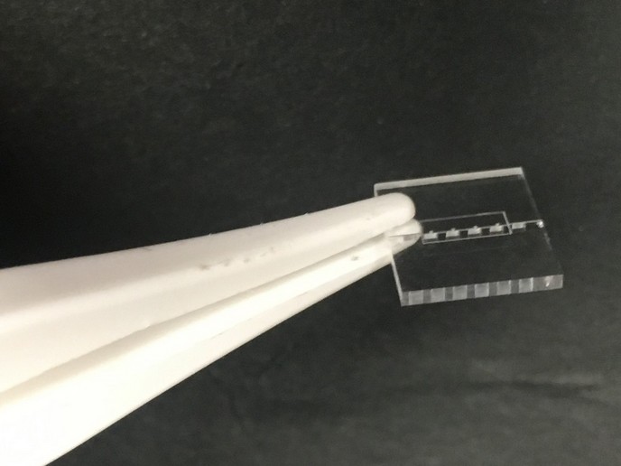
Thin-film solar cells based on an absorber layer of Cu(In,Ga)Se2, so-called CIGS, offer low weight, low-light efficiency, flexibility, competitive production costs and, importantly, good aesthetics. The EU-funded ARCIGS-M(opens in new window) project is working to capitalise on this potential by developing advanced solar cell architectures. The ultimate aim is to further drive down the production costs of CIGS solar modules. Single-step, silver-laced production “The ARCIGS-M project focuses on low-cost thin-film solar cells with very high efficiency suitable for integration in buildings,” project coordinator Prof. Marika Edoff sums up. “We use two types of substrates, either ordinary soda-lime glass or low-cost steel substrates.” A layer of electric insulation is used to coat the steel substrates, enabling single-step production of solar-cell modules without the need for soldering single cells. All thin-film solar cells consist of two contacts: an absorber layer, where sunlight is absorbed, and a transparent front contact. The absorber layer in ARCIGS-M solar cells consists of CIGS, a semiconductor material with a direct band gap. The band gap is a material property and corresponds to the minimum photon energy (from sunlight) required to excite an electron. However, in materials with direct band gap, the absorption has a very high probability and therefore allows for very thin layers of just a few micrometres. ARCIGS-M targets a thickness of only 0.5 µm. The professor notes: “This is not enough for full absorption. Therefore, we have changed our back contact from a layer of molybdenum to a multilayer stack with silver, which provides very high reflectivity, close to 90 %.” Ongoing achievements Among the project’s main achievements, one of the most important is the back-reflector layer, “that we have proven works well together with the CIGS layers,” Prof. Edoff says. To prevent the loss of electrons from the back contact, a layer of a passivating material is added that consists of aluminium oxide perforated with nano-sized openings. “Patterning of the back-contact passivation layer is done in nano-scale with nano-imprint lithography, a method that we show to be scalable for this type of device for the first time,” the coordinator reports. The team has also developed an opto-electric model that is used to provide feedback. Beyond tech developments Notably, the project is making strides outside the lab too. “We have strived to achieve a good gender balance in a field that traditionally is strongly dominated by men,” Prof. Edoff states. The project’s coordinator and co-coordinator are both women, “and for the total project we have managed to get about 40 % female participants in the meetings.” “We hope our project will contribute to new business opportunities for our partners who come from many different complementary fields,” Prof. Edoff comments. These include a utility company, a steel manufacturer and equipment manufacturers. A quote from a 2018 interview(opens in new window) sums up the professor’s vision: “Photovoltaics is the present and the future! It is the most democratic way of generating electric power.”